CIOE2026-visit-notes.md in any Markdown editor; photos are in images/. The original Chinese notes are included as well.On-site notes taken 2026-09-11 at CIOE 2026 (Shenzhen World Exhibition & Convention Center), organised by vendor. Photos are in
images/.
This year's highlight: waveguide gratings made directly by DUV lithography, replacing the nanoimprint (NIL) route.
Process difference (as explained at the booth):
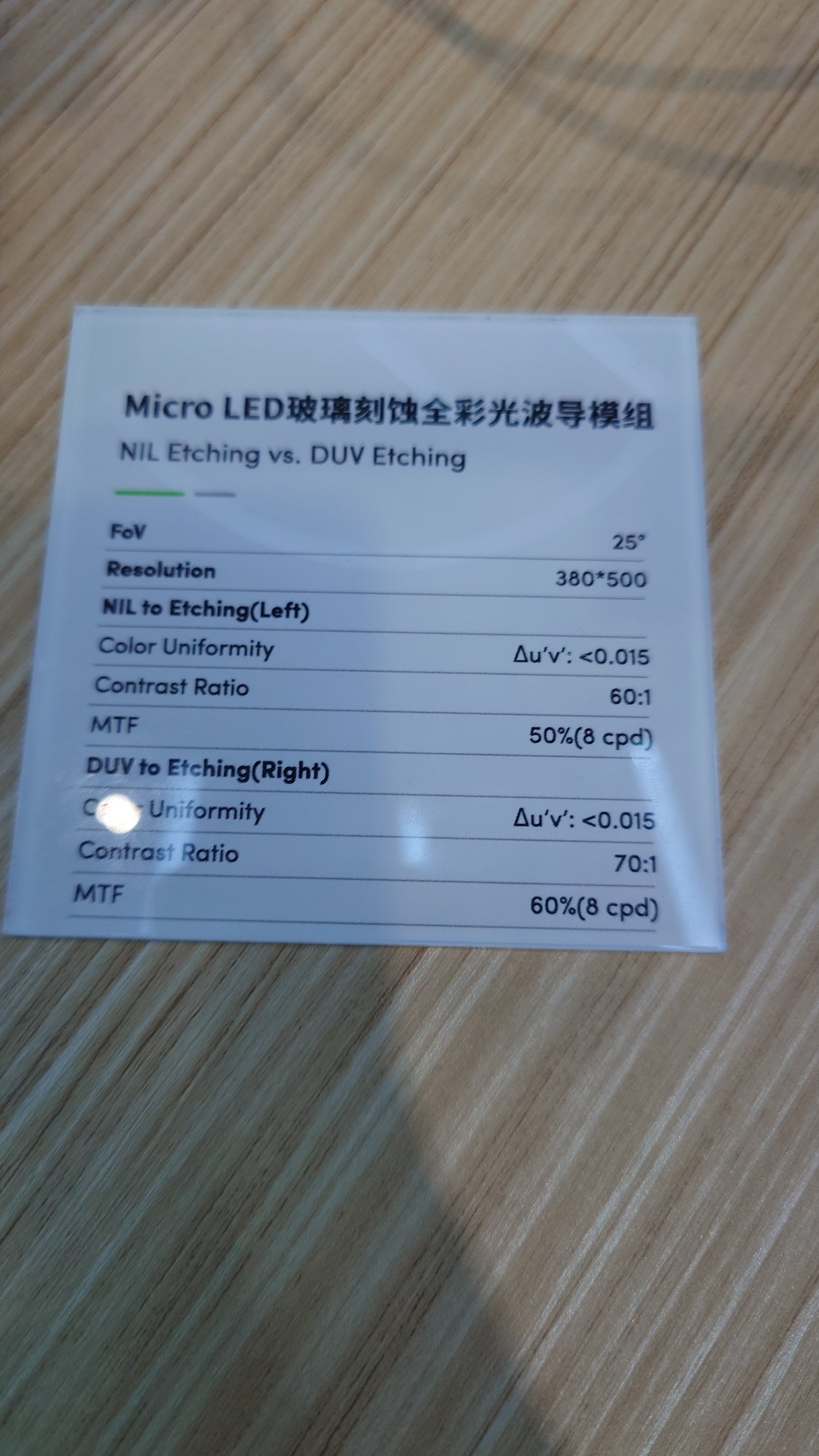
Exhibit: Micro LED glass-etched full-colour waveguide module. One spec card compares NIL etching (left eye) and DUV etching (right eye) side by side:
| Item | NIL Etching (left) | DUV Etching (right) |
|---|---|---|
| FoV | 25° | 25° |
| Resolution | 380×500 | 380×500 |
| Colour uniformity | Δu'v' < 0.015 | Δu'v' < 0.015 |
| Contrast ratio | 60:1 | 70:1 |
| MTF | 50% (8 cpd) | 60% (8 cpd) |
The DUV-etched version measures better: contrast 70:1 vs 60:1, MTF 60% vs 50%; colour uniformity is the same.
Key point: their AR waveguides do not use the common SRG (surface-relief grating). They use PVG (Polarization Volume Grating), fabricated from liquid crystal.
Asked how PVG differs from a conventional surface-relief grating, the booth answered:
The catalogue also lists photopolymer materials and array (geometric) waveguide modules, but PVG is the main product.
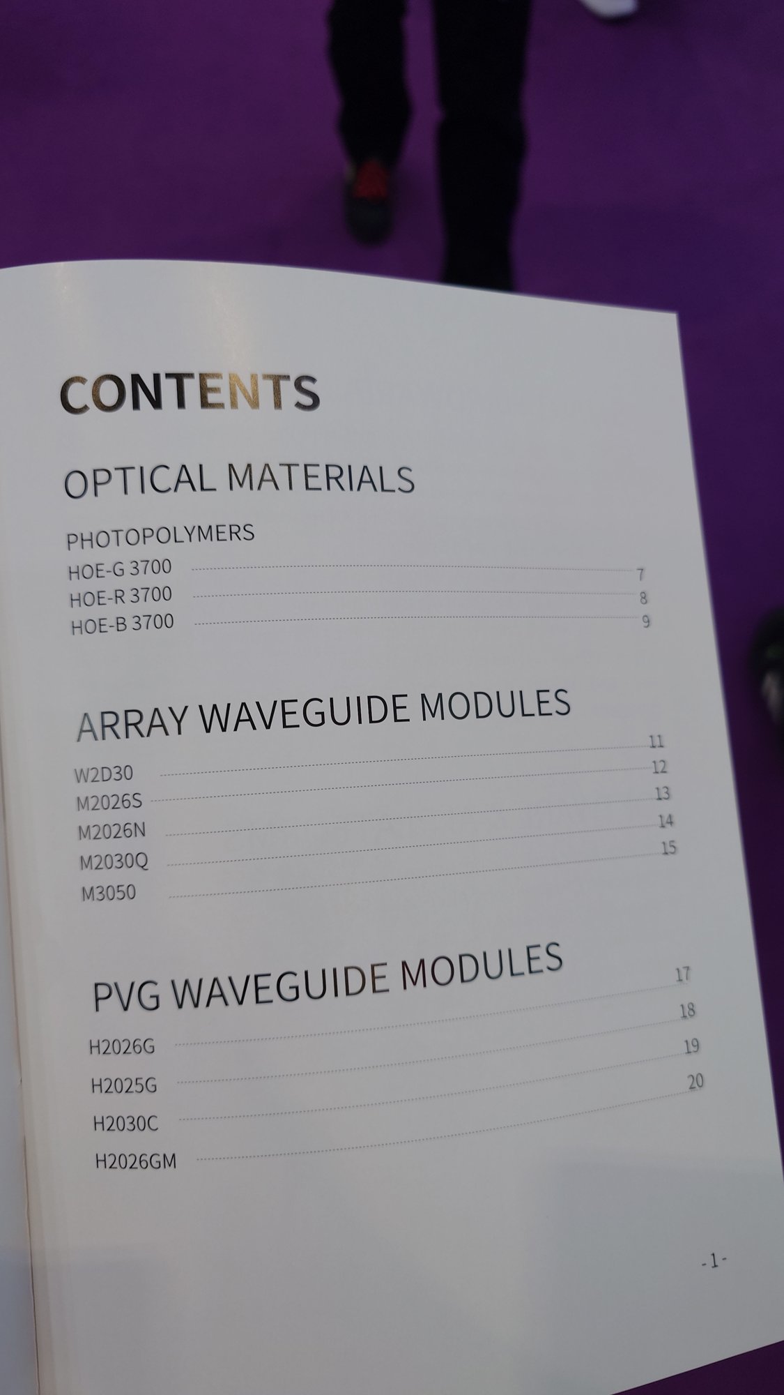
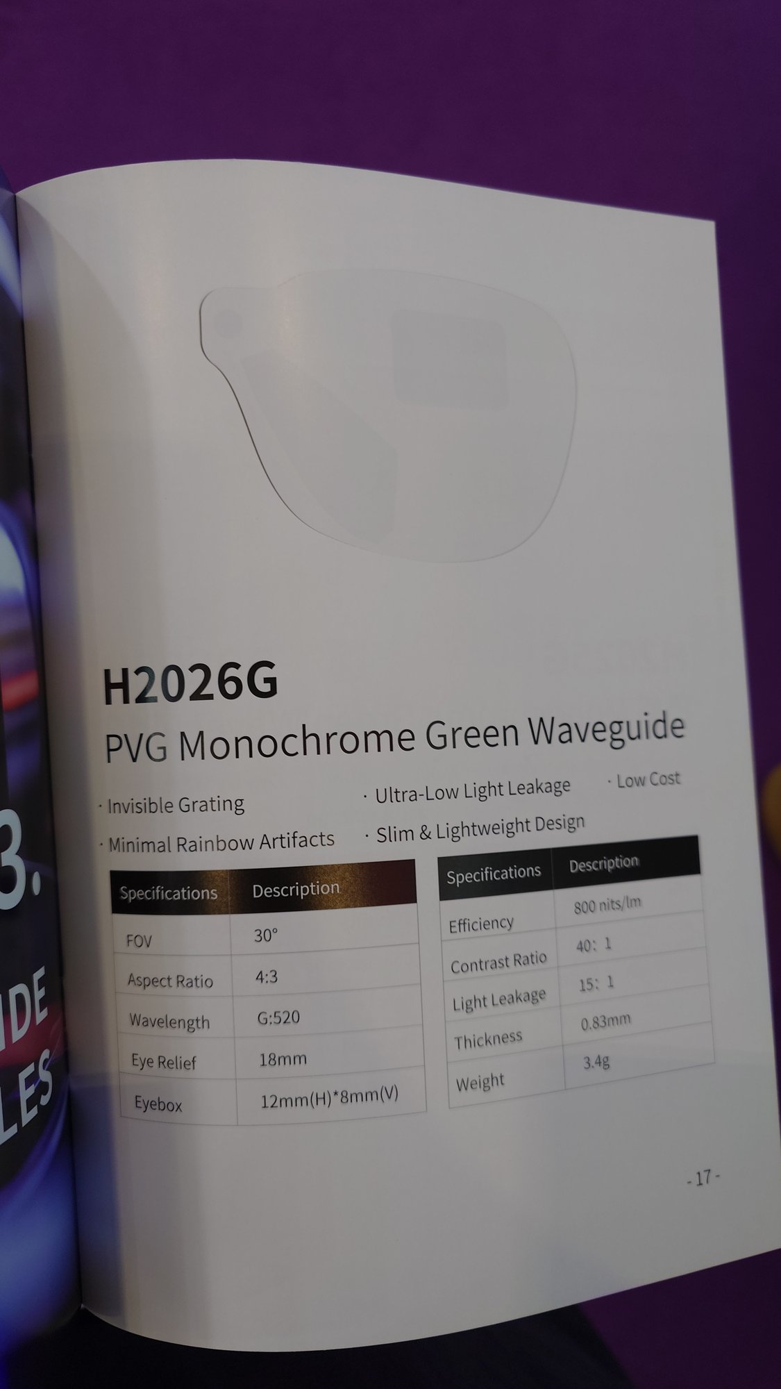
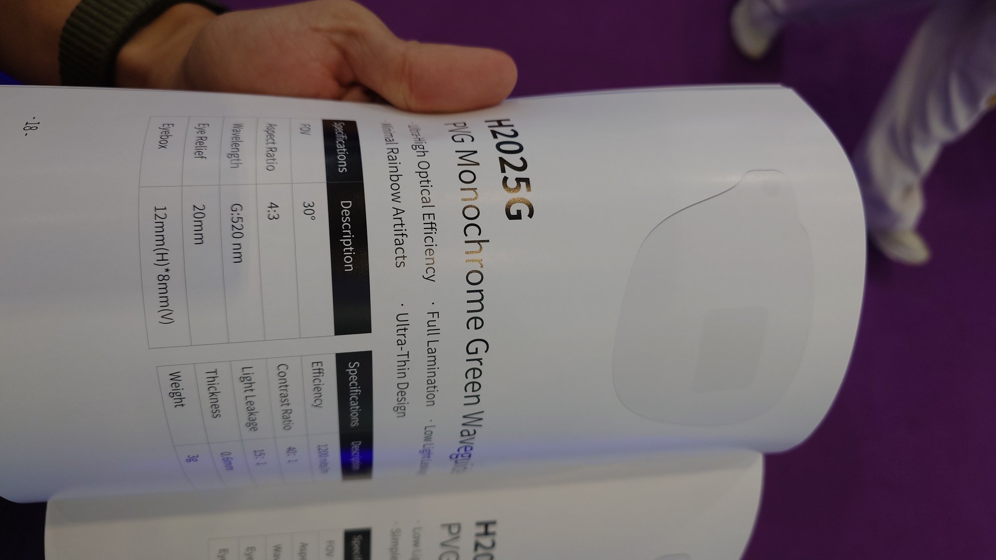
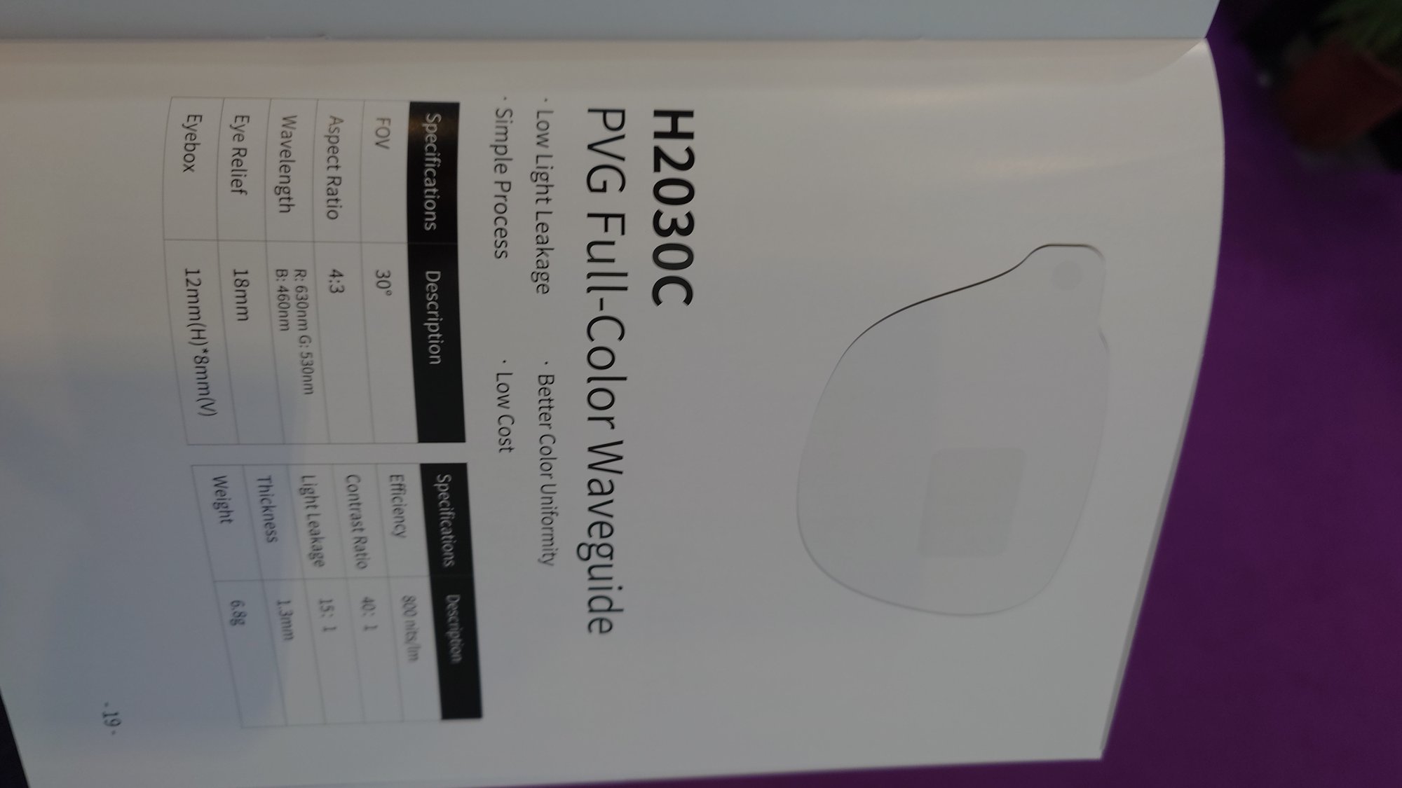
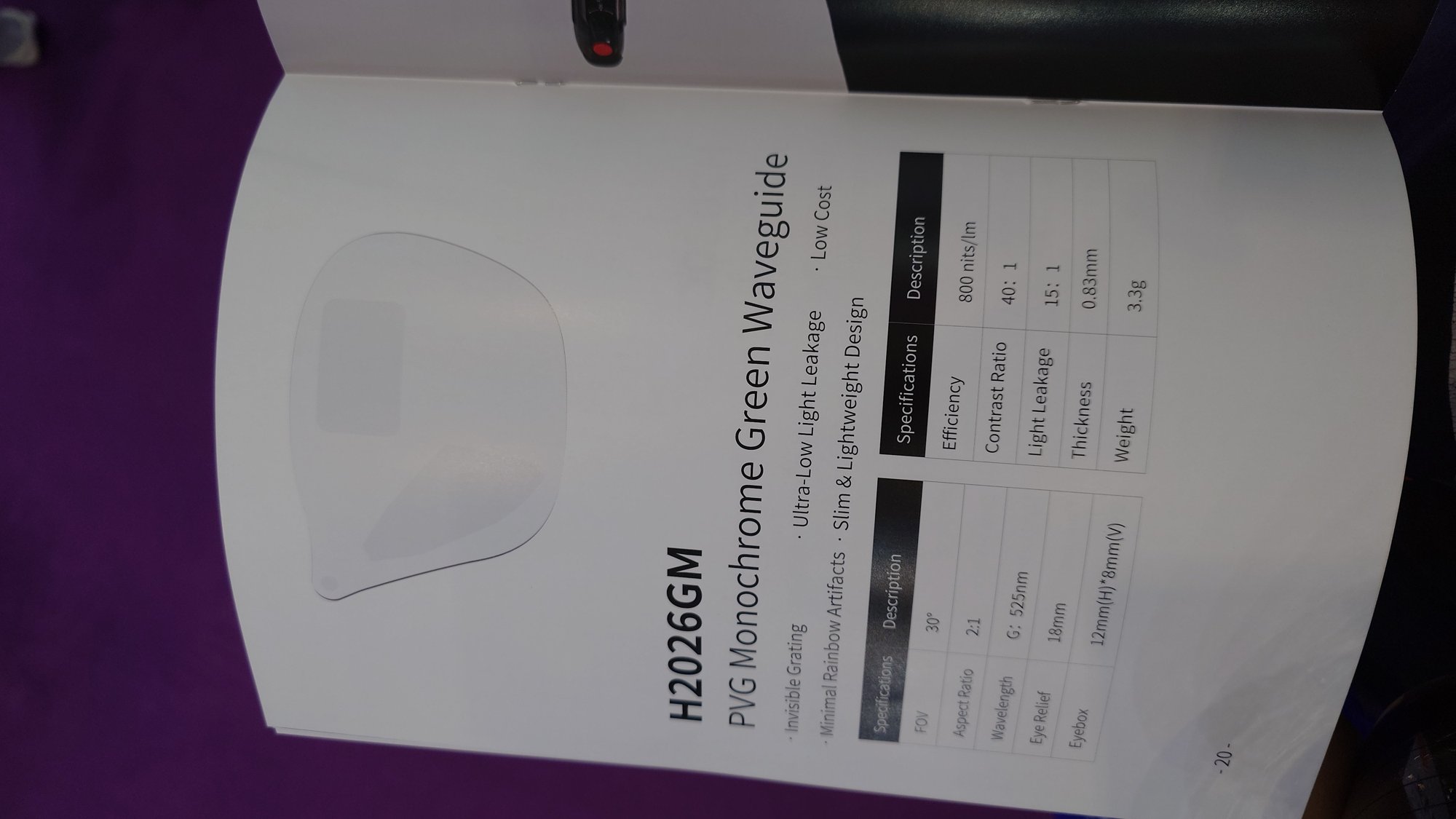
Catalogue contents, three product families:
PVG waveguide modules, four models (catalogue pp. 17–20):
| Item | H2026G | H2025G | H2030C | H2026GM |
|---|---|---|---|---|
| Type | Mono green | Mono green | Full colour | Mono green |
| FoV | 30° | 30° | 30° | 30° |
| Aspect ratio | 4:3 | 4:3 | 4:3 | 2:1 |
| Wavelength | G: 520 nm | G: 520 nm | R: 630 / G: 530 / B: 460 nm | G: 525 nm |
| Eye relief | 18 mm | 20 mm | 18 mm | 18 mm |
| Eyebox | 12 (H) × 8 (V) mm | 12×8 mm | 12×8 mm | 12×8 mm |
| Efficiency | 800 nits/lm | 1200 nits/lm | 800 nits/lm | 800 nits/lm |
| Contrast ratio | 40:1 | 40:1 | 40:1 | 40:1 |
| Light leakage | 15:1 | 15:1 | 15:1 | 15:1 |
| Thickness | 0.83 mm | 0.6 mm | 1.3 mm | 0.83 mm |
| Weight | 3.4 g | 3 g | 6.8 g | 3.3 g |
Marketing points: all four stress minimal rainbow artifacts, low light leakage and low cost. H2026G / H2026GM add "invisible grating" and "slim & lightweight"; H2025G is positioned on ultra-high optical efficiency (1200 nits/lm), full lamination and ultra-thin design (0.6 mm); H2030C (full colour) claims a simple process and better colour uniformity.
The booth also mentioned that the grating is written by two-beam interference, and that the liquid crystal aligns itself according to the interference field.
Typical three-step flow:
So "the LC aligns itself to the light field" is roughly right, but more precisely: the interference exposure records a polarisation pattern in the surface alignment layer, and the LC then self-assembles on that template and extends it into the bulk via the chiral dopant. The intuition that "the surface needs a guiding structure" is also correct — the guide is just a photo-alignment layer rather than a relief structure. Curing is UV polymerisation. Literature reports diffraction efficiencies above 80% for RGB PVGs.
References: SEU / Optics Letters: LC-based PVG for full-colour waveguide displays, Reflective PVG for high-efficiency waveguide-coupling AR displays, MDPI: FoV performance of full-colour waveguide displays based on PVG
Observation: a surprisingly large number of exhibitors make reflective (array) waveguides. The technology itself is easy to understand and there was not much hidden detail. After talking to several of them, the process is confirmed to be: stack multiple glass substrates, each interface carrying its own (partially reflective) coating, bond them, then cut at an angle. The challenge is essentially all on the manufacturing side (coating and stack/cut precision, yield).
1D and 2D array waveguide modules:
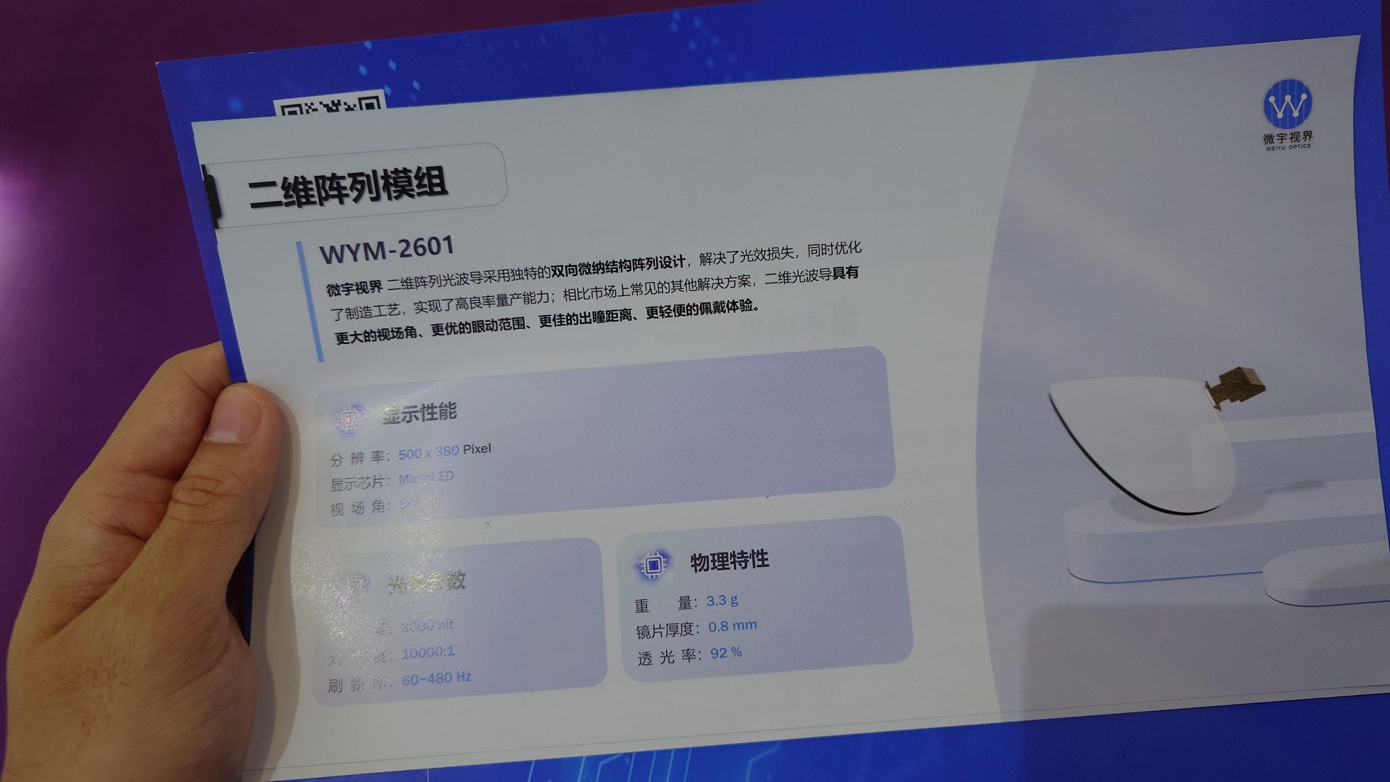
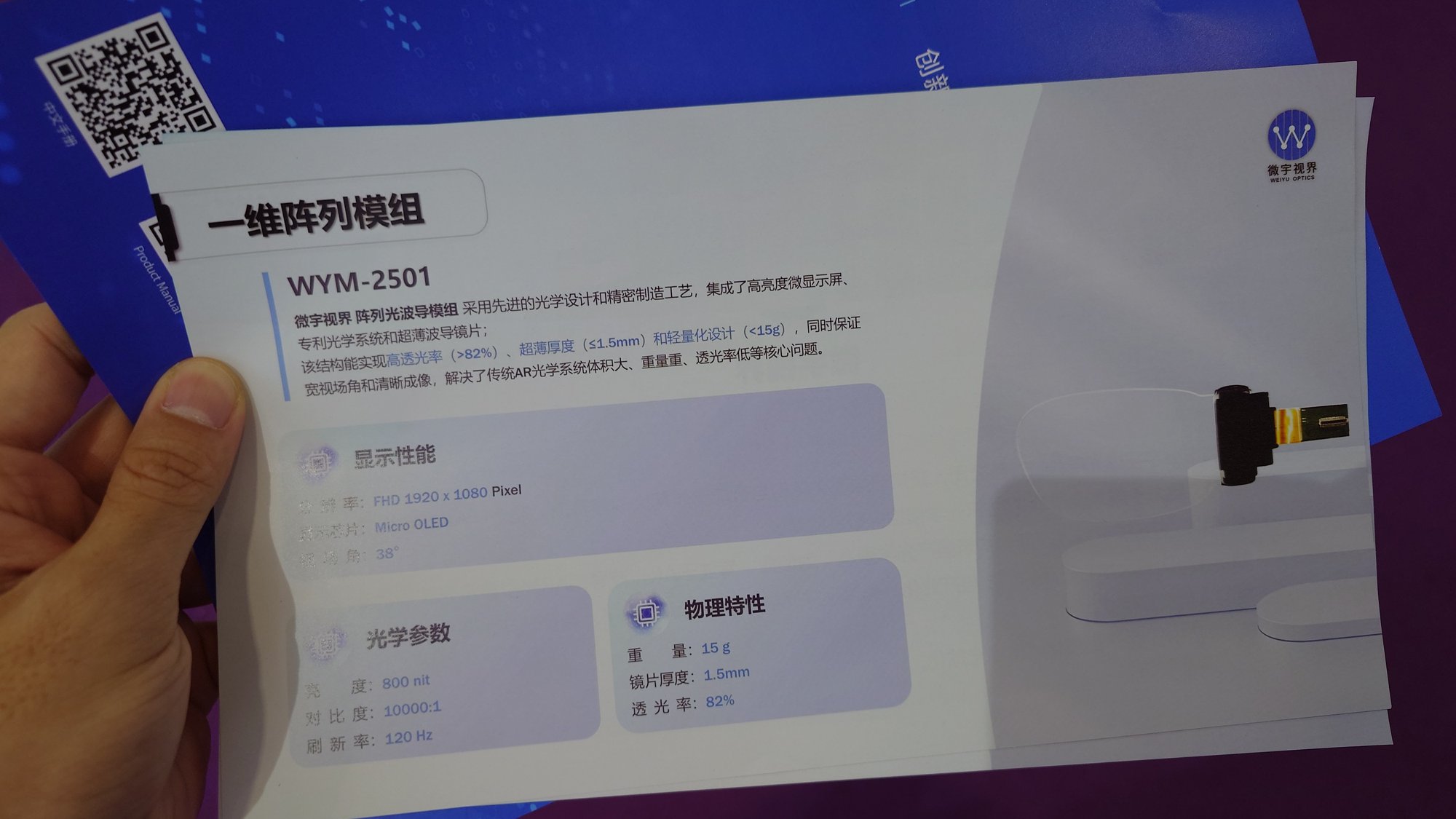
| Item | WYM-2501 (1D array) | WYM-2601 (2D array) |
|---|---|---|
| Display | Micro OLED | MicroLED |
| Resolution | FHD 1920×1080 | 500×380 |
| FoV | 38° | (glare on the flyer, not readable) |
| Brightness | 800 nit | 3000 nit |
| Contrast | 10000:1 | 10000:1 |
| Refresh rate | 120 Hz | 60–480 Hz |
| Lens thickness | 1.5 mm | 0.8 mm |
| Weight | 15 g | 3.3 g |
| Transmittance | 82% | 92% |
WYM-2601 (2D array) copy: a proprietary bidirectional micro/nano structure array design that addresses optical efficiency loss, with an optimised process for high-yield mass production; compared with other solutions it claims larger FoV, better eyebox, better eye relief and lighter weight.
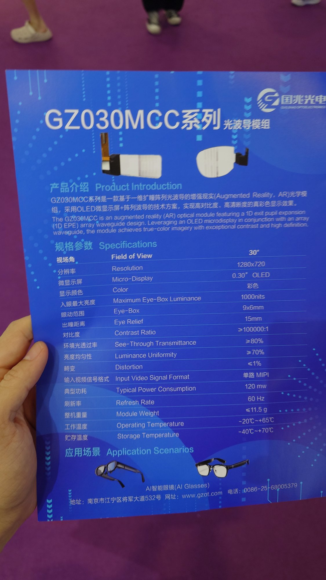
GZ030MCC series: AR module combining a 1D exit-pupil-expansion (1D EPE) array waveguide with a 0.30" colour OLED microdisplay, aimed at AI smart glasses.
FoV 30°, 1280×720, max eyebox luminance 1000 nits, eyebox 9×6 mm, eye relief 15 mm, contrast ≥100000:1, see-through transmittance ≥80%, luminance uniformity ≥70%, distortion ≤1%, single-lane MIPI, typical power 120 mW, 60 Hz, module weight ≤11.5 g, operating temperature −20 to 65 °C. (Jiangning District, Nanjing; gzot.com)
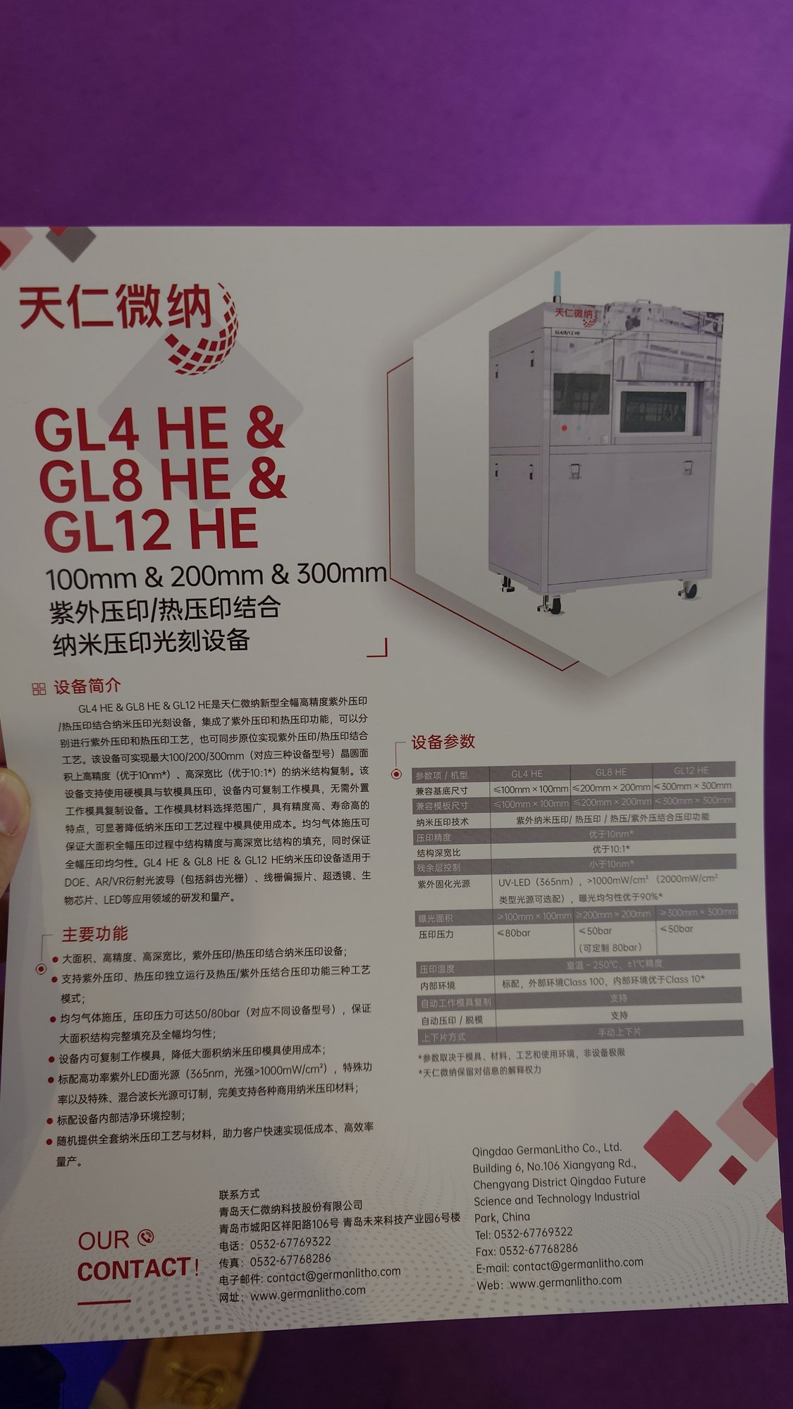
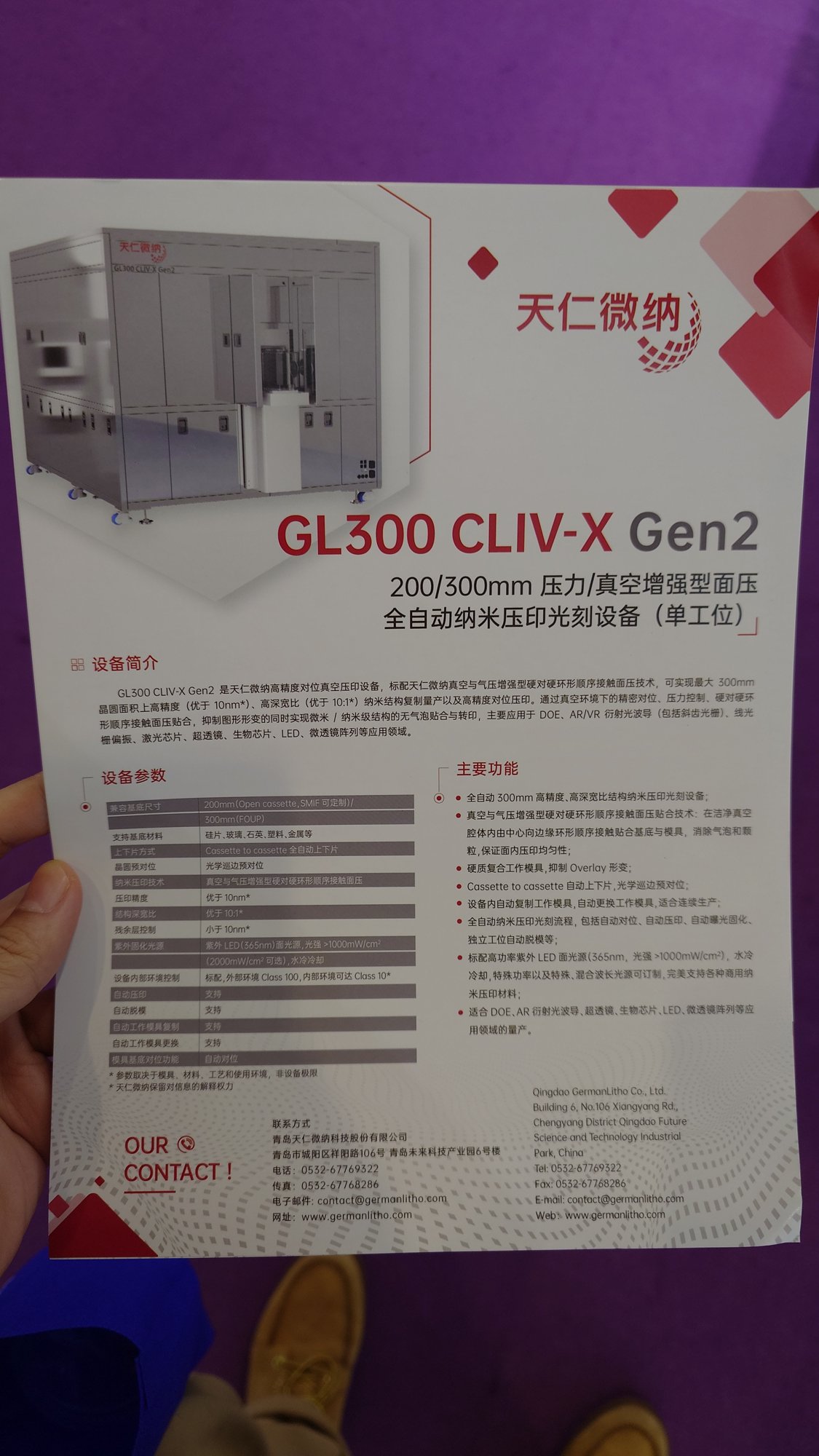
Nanoimprint lithography (NIL) equipment maker. Wandered in without a plan; nothing particularly unusual. Asked how the master is made: either photolithography or EBL.
Two equipment flyers:
(Qingdao GermanLitho Co., Ltd., germanlitho.com)
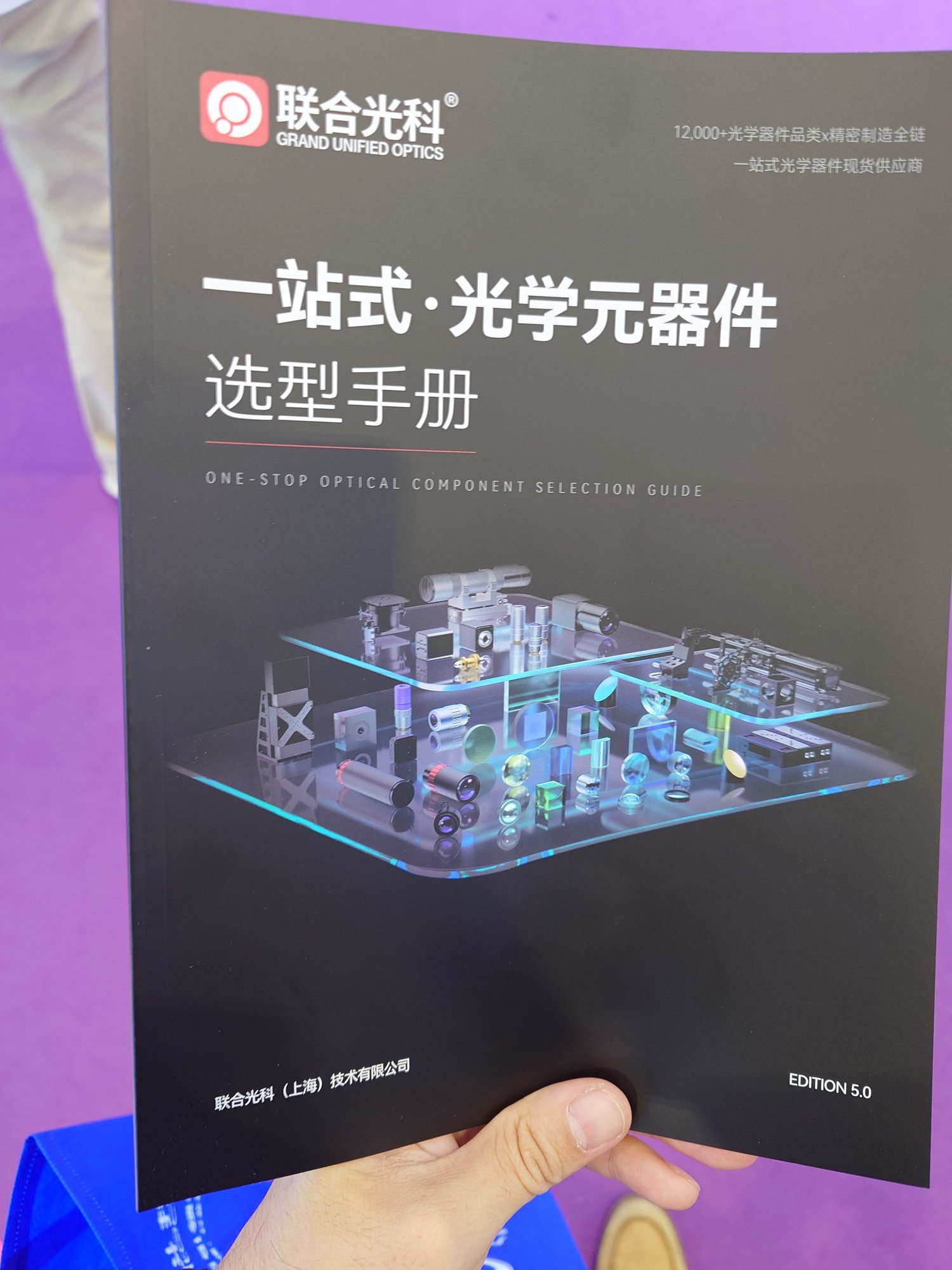
A catalogue handed out in the aisle ("One-Stop Optical Component Selection Guide", Edition 5.0). An optics "general store" selling off-the-shelf components: 12,000+ SKUs, in-house precision manufacturing, one-stop stock supply — lenses, prisms, filters, stages, mounts for lab and system-integration use. Business model similar to Thorlabs / Edmund Optics (a Chinese peer is Daheng Optics).
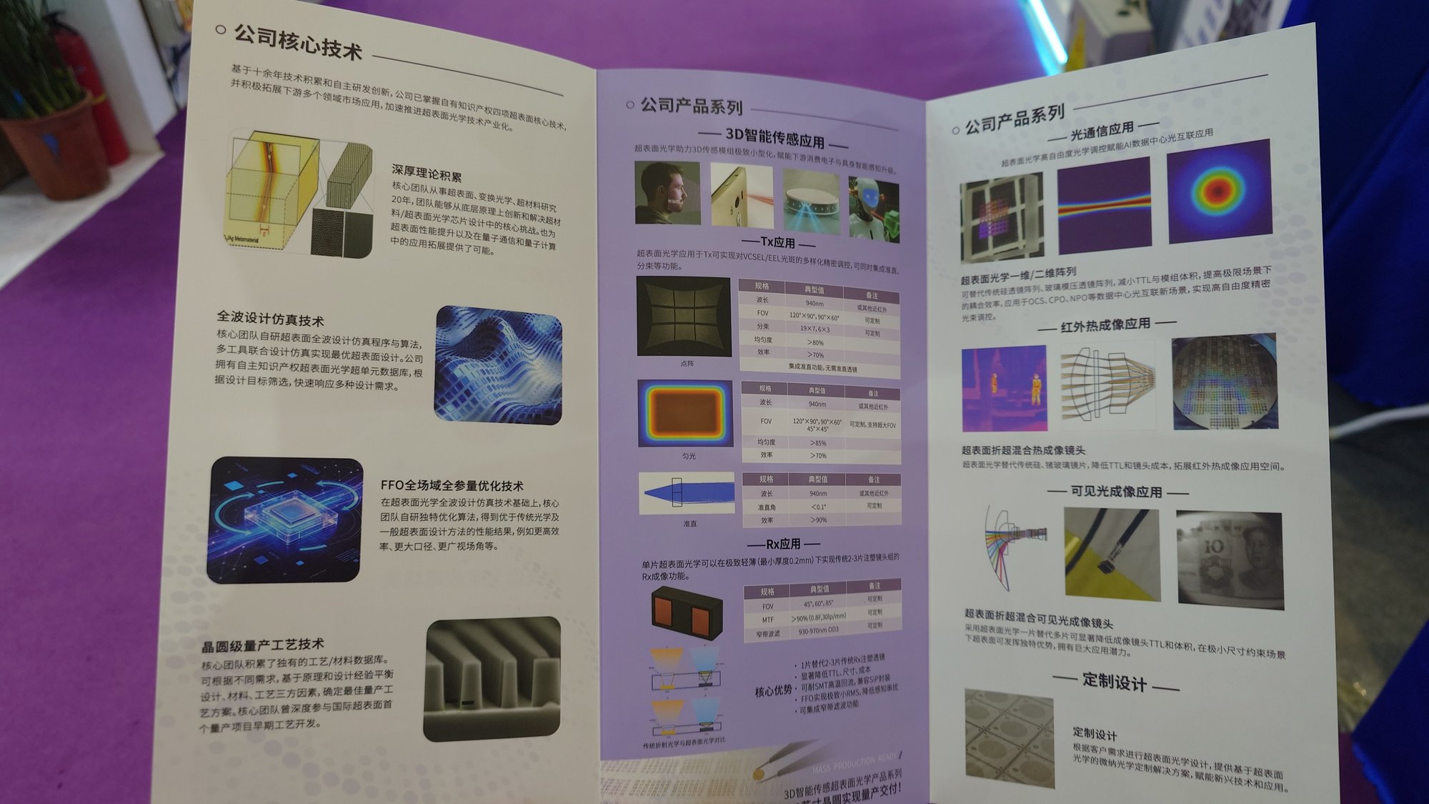
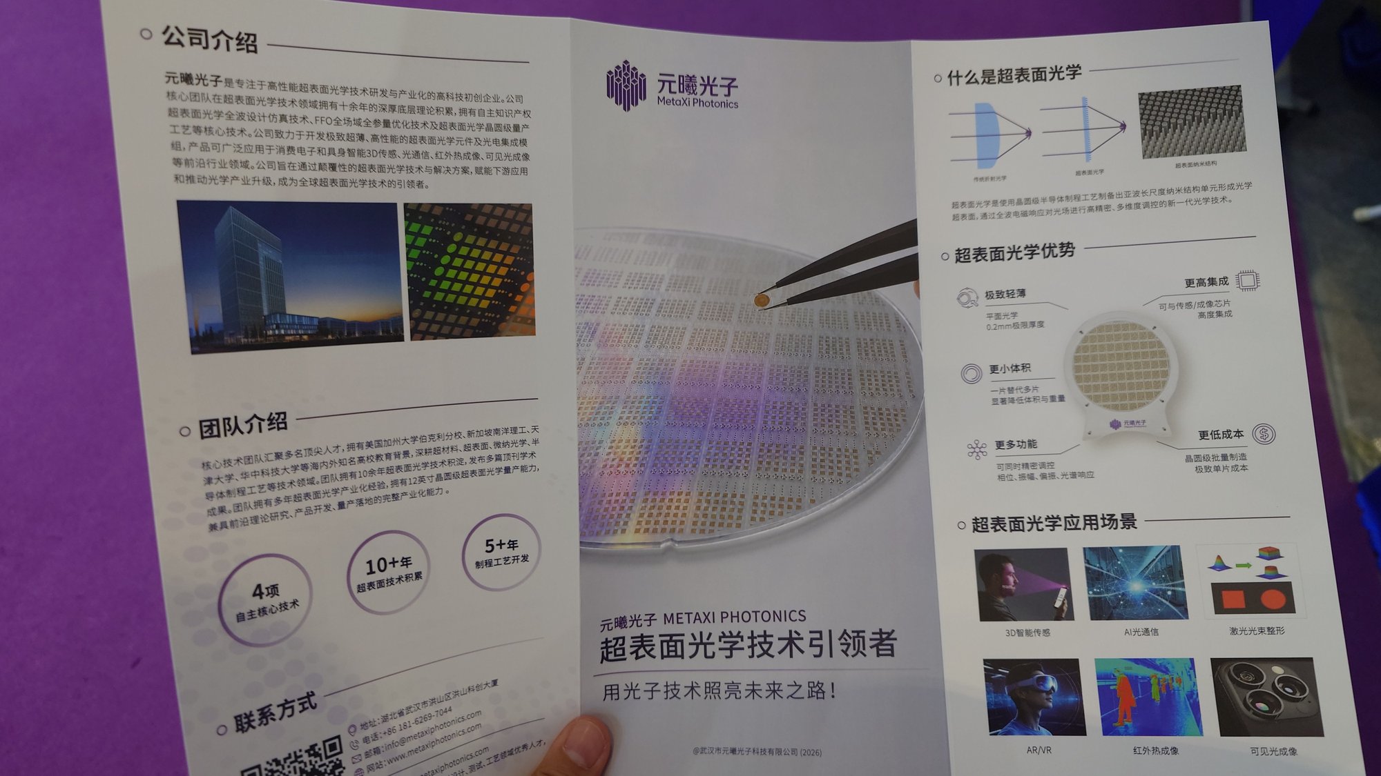
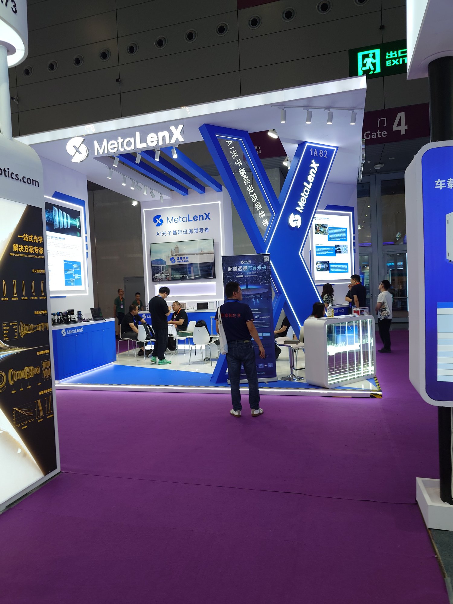
Metalens company; booth slogan "AI photonics infrastructure leader". Impression after the conversation: a fairly complete product line, with products already in mass production.
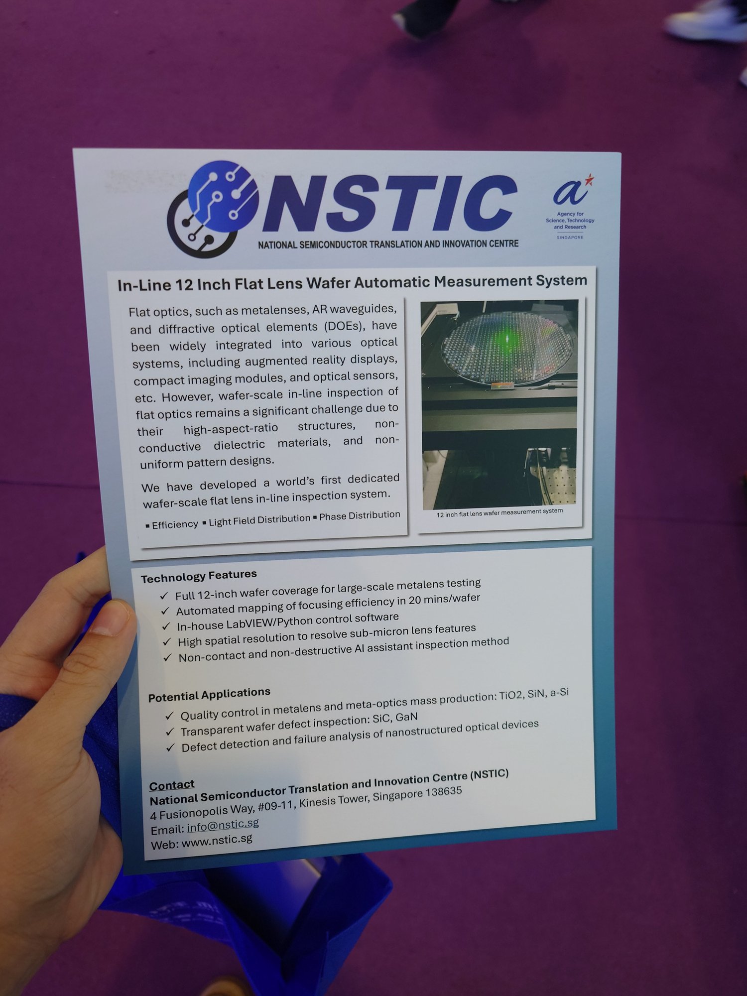
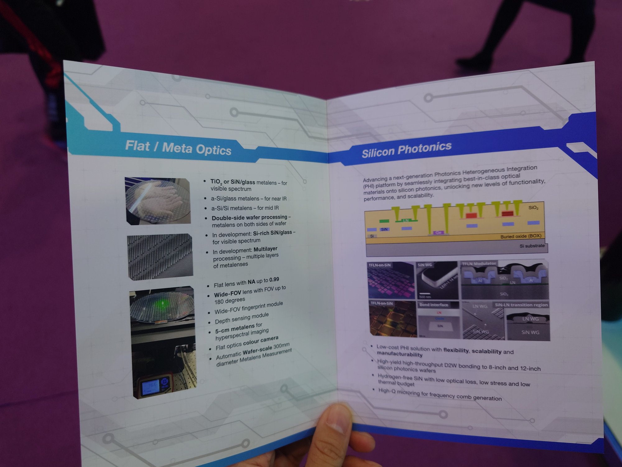
NSTIC (National Semiconductor Translation and Innovation Centre) under Singapore's ASTAR. On display: a 5 mm visible-light metalens and a 5 cm mid-IR metalens* (the flyer lists the 5-cm metalens for hyperspectral imaging).
Flat / Meta Optics platform (flyer highlights):
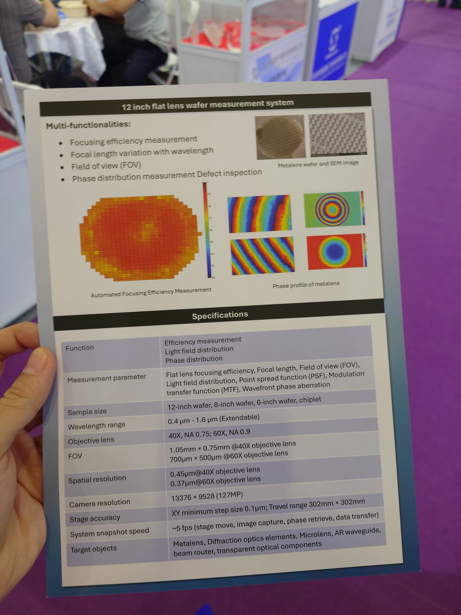
In-line 12-inch flat lens wafer automatic measurement system (claimed to be the world's first dedicated wafer-scale flat-lens in-line inspection system):
The other page covers Silicon Photonics: a PHI heterogeneous-integration platform (TFLN-on-SiN, 8/12-inch D2W bonding, hydrogen-free low-loss SiN, high-Q microrings for frequency combs) — off-topic for this visit, noted for completeness.
Metasurface optics start-up (12-inch wafer-level mass-production capability; team background UC Berkeley, NTU Singapore, Tianjin University, HUST). Talked to them but did not learn much; two key points:
Catalogue summary: